Introduction
With increasing demand of LCD panel for high color depth and resolution it is hard to design a buffer with high resolution. The buffer has to match the speed, resolution, voltage swing and power dissipation of an LCD driver’s to get high resolution. The resolution of the amplifier is dependent on the settling time the offset voltage and the slew rate.
The offset voltage is caused by the mismatch of the devices used in the circuit which limits the high-resolution of LCD driver. The general technique used to reduce the offset voltage is the output offset storage technique and input offset storage technique. However these two techniques introduce capacitors in the signal flow path. This is a serious issue in operational amplifiers and feedback systems. Parasitic capacitors thus formed can cause degradation of phase margin of the circuit thereby reducing stability of the circuit. So we have to design a circuit in such a manner that the offset cancellation technique should not come in the way of signal flow path.
We generally design a buffer with push-pull output stage which consists of two complementary common source transistors allowing RAIL TO RAIL output voltage swing. The gates of two output transistors can be driven by two in phase AC signals separated by DC voltage. In this paper single ended amplifiers are used to drive the two output devices to achieve offset cancellation and to drive push-pull output. We use class AB operation because no extra current paths are needed in this operation.
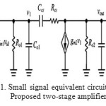
The equivalent circuit of the proposed two-stage amplifier is shown in Fig.1, where gm1 and gm2 , R01 and R02, and C01 and C02 are the transconductances, output resistances, and output parasitic capacitances of the first-stage and second-stage amplifiers, respectively. CCS and RCS are used for the stability of the circuit. The data line of the LCD panel is an R-C distribution. To simplify the small-signal analysis, the data line is modeled as a first-order R-C circuit. Since the first stage amplifier contains dual complementary differential pairs, the value of gm1 depends on the input common-mode voltage.
Design Issues
To evaluate this value of gm1 ,the input voltage is divided into low, middle, and high levels. When the input voltage is at the low level, the PMOS input transconductance amplifiers are operating and the NMOS input transconductance amplifiers are cut off, vice versa for the high-level inputs. All transconductance amplifiers can amplify the input signal when the input voltage is at the middle level. Hence, the value of gm1 can be expressed as
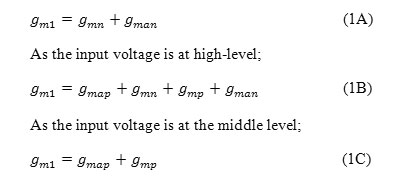
As the input voltage is at a low level in equation (1) where gman, gmp, gmap, gmn are the transconductance amplifiers Gmap, Gmn, Gman, Gmp respectively. Since the transconductance of the first stage amplifier varies with the input common-mode voltage, the dc gain of the amplifier varies over the signal swing for large signals. The distortion will then be generated in a continuously large signal. To reduce the distortion encountered due to this variation, the input stage should be modified to a rail-to-rail constant gm differential amplifier. For an LCD driver application, the amplifier is used to buffer the step-wise signals. Hence, the constant gm design is not suitable.
The open-loop transfer function AO(s) can be obtained from Fig. 2 and the assumptions:
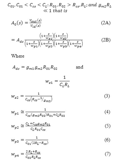
The zeros at wz1 and wz2 are contributed by the distributed load and the Miller compensation, respectively. The dominant pole wp1, is due to the Miller compensation and the distributed R-C load. The first term of the denominator in (4) is arisen at the interface between the first and second stages. The output resistance of the first stage,R01, is interacting with the Miller capacitance,CCSgm2R02 at the interface. The second term is due to the output resistance of the second stage and the load capacitance. Since the load capacitance of the LCD data line can be the order of hundred pico-farads, the second term,CLR02 , cannot be neglected in the LCD driver application.
The second non-dominant pole wp2 is arisen at the output of the second stage amplifier with the Miller effect. For a conventional two-stage operational amplifier, the first term of the numerator in (5) is much smaller than the second one, resulting to that
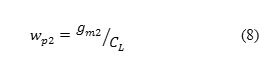
That is: wp2 is determined by the trasnconductance of the second stage amplifier and the load capacitance. Here, for the LCD driver application, the load capacitance cannot be neglected. If is much greater than CCSgM2R01 , wp2 can be approximately expressed as: 1/CCSR01 , which is independent on the transconductance of the second stage amplifier and the load capacitance.
The third and fourth nondominant poles wp3 and wp4 due to the parasitic capacitances, are far away from the other poles and zeros. Hence, they have less effect on the stability. The unity-gain frequency can be approximately expressed as
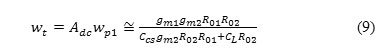
which is larger than the second pole
Hence, the actual value of the unity-gain frequency is slightly smaller than that of (8). The position of wz1 is greatly affected by the R-C load.
The larger the load connected to the amplifier, the smaller the value of wz1 decreasing to less than the unity-gain frequency for a large load.
Proposed Amplifier Design
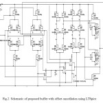
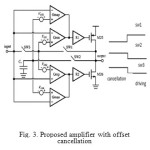
The auxiliary transconductance amplifiers are used to extend the input swing. They can also be used for the offset cancellation. The architecture of the proposed amplifier without an offset cancellation is shown in Figure 2, and The architecture of the proposed amplifier with an offset cancellation is shown in Fig 4.4 where an offset storage capacitor and three switches are used in the circuit, andVOS1, VOS2, VOS3 and VOS4 are the input-referred offset voltages of Gmap, Gmn, Gman, Gmp respectively.
Since the input stage contains both PMOS and NMOS differential amplifiers, the offset voltage varies with the input voltage. For the LCD driver application, a step-wise signal is applied to the input of the buffer amplifier. Hence, the buffer amplifier must sample each voltage level for the offset cancellation. The operation is divided into offset cancellation and driving phases. Before each driving phase, the amplifier is in the offset cancellation phase, the switches SW2 and SW3 are turned on, and the switch SW1 is turned off. After the offset cancellation is finished, SW1 is turned on and SW2 and SW3 are turned off. The circuit is then ready to drive its load.
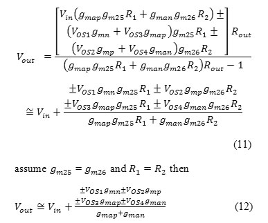
During the offset cancellation phase, a negative feedback loop consisting of the auxiliary transconductance amplifiers, Gmap and Gman the transimpedance amplifiers, R1 and R2, and the output transistors, M25 and M26, is formed. The input voltage is applied to the inverting input terminals of all transconductance amplifiers and to the non-inverting input terminals of the two main transconductance amplifiers. As depicted in Fig. 3, the input-referred offset voltages VOS1 and, VOS2 are applied to the two inputs of Gmn and Gmp , respectively. The relation between the input and output voltages can be expressed as
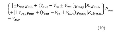
where gm25 and gm26 are the transconductances of M25 and M26, respectively, and Rout is the output resistance of the amplifier.
assume gm25 = gm26 and R1 = R2 then
When SW2 andSW3 were off and SW1 is on the output voltage is stored at the capacitance called as output offset voltage is
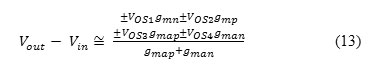
The total output of the voltage referred to the input is given as
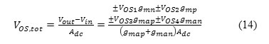
Where ADC is the DC gain of amplifier of the order of 80 dB. The switch SW2 will introduce injection induced either with generate, input referred offset voltage expressed as
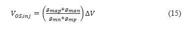
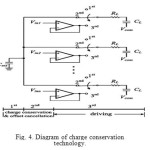
Where ∆V is the injection induced error on the storage capacitor to reduce the center the transconductance of the main transconductance amplifier is designed to be higher than auxiliary transconductance amplifier. In this methodology charge conservation technology is used to reduce the power consumption. In this process the data line are divided into three phase as in first phase all data lines are isolated from the output of the buffers. In second phase they are shorted with external capacitor, this two phases are used to conserve charge on data line in last phase all data lines connected with output buffer to drive the data line to their final values. This charge conservation is used for offset cancellation, and it eliminates the need of additional phase consideration for the buffer amplifier means the driving time does not need to be elongated.
Charge conservation technology, which is shown in Fig.4, is usually used to reduce the power consumption by reducing the average voltage swing. The voltage level refresh of the data lines is divided to three phases. In the first phase, all data lines are isolated from the outputs of the buffers. In the second phase, they are shorted to an external capacitor Cext. These first two phases are used for the charge conservation of the data lines. In the last phase, all data lines are connected to their corresponding buffer amplifiers, and the buffer amplifiers continue to drive the data lines to their final values. The charge conservation phase can also be used for the offset cancellation of the proposed amplifier, eliminating the need for an additional phase for offset cancellation. Thus, the driving time does not need to increase.
Design Process of Buffer
(A) Design Process (1/3)
Model Parameter Extraction
- kn ,kp
- λn ,-λp
- Vthn ,Vthp
all these can be get by process technology
Assign Current from Power Consumption Spec.
- Total Current : 3I mA
- Input pair : I mA
- Current mirror : 2I mA
(B) Design Process (2/3)
- Determine W3 from CM_min, CM_max Spec.
- CM_min
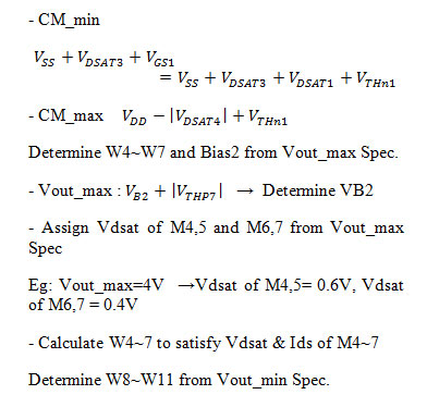
- Assign Vdsat of M8~M11 from Vout_min Spec.
Eg) Vout_min=0.8V →Vdsat of M8~11 = 0.4V
- Calculate W8~11 to satisfy Vdsat and Ids of M8~11
Design Process (3/3)
Determine W1,2 from Gain Spec.
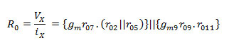
Calculate Rout_total
- Calculate Required Gm value to satisfy Gain Spec.
- Gain = Gm*Rout
- Calculate W1,2 from Gm
- Check other Spec. and Repeat the design process to optimize
transistors size
- Slew Rate
- CM_min Check required
- CMRR, PSRR
- Check and Modify Bias Voltage to optimize transistor size.
Results
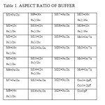
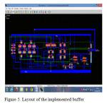
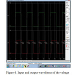
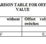
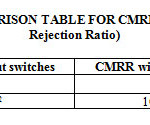
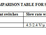
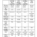
Simulation and results are obtained using LTSPICE & MICROWIND software’s. Results illustrate the tracking behavior of the proposed output buffer driven by a 50-kHz large-swing triangular wave and loaded with a large-size capacitance of 140pF. As can be inspected, the output voltage basically follows the input voltage for a full dynamic range. To show the output driving performance of the discussed buffer, results depicts the simulated transient response to a 50-kHz full-swing input step for the same capacitive load. Slew-rate values are found to be 12V/µs and 14V/µs for the rising and falling edges, respectively, whereas positive and negative settling time values within 1000% of the final output voltage are only 3µs and 3.7µs, respectively. As can be observed, the output waveform follows the input waveform. The major performance parameters of the analyzed buffer are summarized and compared to other conventional topologies in Table 5, which shows a remarkable improvement of the proposed amplifier over other previously reported buffers. Figure 5 shows the layout of the analog buffer manually designed using Microwind. And the next diagram figure 6 shows its timing diagram. We can clearly see that output follows input. Table 2 compares the offset values using offset cancellation technique and without it. The method used for this work makes a huge difference in the offset voltage value. Similarly Tables 3 and 4 show that the inclusion of the three switches does not affect the CMRR and Slew Rate values.
Conclusion and Future Scope
It is limpidly visually perceived in the results that the output waveform follows the input waveform. Withal the comparison table depicts a remarkable amelioration of the proposed amplifier over other antecedently reported buffers. Hence the high speed self inequitable low power rail-to-rail class-AB low offset buffer amplifier is implemented prosperously Since the dissertation topic implements a very compact, high speed rail-to-rail buffer for LCD drivers, it can be utilized as a boon in many future applications where die area is a matter of concern, additionally where slew rates is a matter of concern. Since it utilises a only 0.74 mV of static puissance, hence is having tremendous demand in hundreds of exhibit contrivances applications.
Due its merits, it can be utilized in following areas-
- Since power consumption is low, it has a great future in getting utilized in applications like “ultra low power ADCs”.
- Since it is utilizing AMLCD technology, the exhibit is amended remarkably, hence can be utilized in “image exhibit contrivances, flat panel exhibits etc.
- Due to rail-to-rail input and output cognations, it is greatly utilized in buffered analog clocks .Above are just few examples, but this buffer is having excellent usability in many other areas also.
- As with reduced offset it will be use full for high colour depth LCD panels means resolution of colour will increase significantly
Refrences
- T. Itaku, H. Minamizaki, T. Satio, and T. Kuroda, “A 402-output TFT-LCD driver IC with power control based on the number of colors selected,” IEEE J. Solid-State Circuits, vol. 38, no. 3, pp. 503–510, Mar. 2003.
CrossRef
- J.-S. Kim, D.-K. Jeong, and G. Kim, “A multi-level multi-phase charge-recycling method for low-power AMLCD column drivers,” IEEE J. Solid-State Circuits, vol. 35, no. 1, pp. 74–84, Jan. 2000.
CrossRef
- Y.-S. Son, J.-H. Kim, H.-H. Cho, J.-P. Hong, J.-H. Na, D.-S. Kim, D.-K. Han, J.-C. Hong, Y.-J. Jeon, and G.-H. Cho, “A column driver with low-power area-efficient push-pull buffer amplifiers for active-matrix LCDs,” in IEEE Int. Solid-State Circuits Conf. Dig. Tech. Papers, 2007, pp. 142–143.
CrossRef
- P.-C. Yu and J.-C. Wu, “A class-b output buffer for flat-panel-display column driver,” IEEE J. Solid-State Circuits, vol. 34, no. 1, pp. 116–119, Jan. 1999.
CrossRef
- T. Itakura and H. Minamizaki, “A two-gain-stage amplifier without an on-chip miller capacitor in an LCD driver IC,” IEICE Trans. Fundamentals, vol. E85-A, no. 8, pp. 1913–1920, Aug. 2002.
- C.-W. Lu and K. J. Hsu, “A high-speed low-power rail-to-rail column driver for AMLCD application,” IEEE J. Solid-State Circuits, vol. 39, no. 8, pp. 1313–1320, Aug. 2004.
CrossRef
- C.-W. Lu and C. L. Lee, “A low power high speed class-AB buffer amplifier for flat panel display application,” IEEE Trans. VLSI Syst., vol. 10, no. 2, pp. 163–168, Apr. 2002.
CrossRef
- Gordon and F. Dingwall, “Matrix addressed LCD display having LCD age indication, and autocalibrated amplification driver, and a cascaded column driver with capacitor-DAC operating on split groups of data bits,” U.S. Patent 5,739,805, Apr. 14, 1998.
- M. J. Bell, “An LCD column driver using a switch capacitor DAC,” IEEE J. Solid-State Circuits, vol. 40, no. 12, pp. 2756–2765, Dec. 2005.
CrossRef
- M. J. Bell, “An LCD column driver using a switch capacitor DAC,” in IEEE Int. Solid-State Circuits Conf. Dig. Tech. Papers., Feb. 2005, pp. 556–557.
CrossRef
- J.-S. Kang, J.-H. Kim, S.-Y. Kim, J.-Y. Song, O.-K. Kwon, Y.-J. Lee, B.-H. Kim, C.-W. Park, K.-S. Kwon, W.-T. Choi, S.-K. Yun, I.-J. Yeo, K.-B. Han, T.-S. Kim, and S.-I. Park, “A 10b driver IC for a spatial optical modulator for full HDTV applications,” in IEEE Int. Solid-State Circuits Conf. Dig. Tech. Papers., Feb. 2007, pp. 138–592.
CrossRef
- R. Ito, T. Itakura, and H. Minamizaki, “A class AB amplifier for LCD driver,” in 2007 Symp. VLSI Circuits Dig. Tech. Papers, Jun. 2007, pp. 148–149.
- A New Compact Low-Power High-Speed Rail-to-Rail Class-B Buffer for LCD Applications Davide Marano, Gaetano Palumbo, Fellow, IEEE, and Salvatore Pennisi, Senior Member, IEEE JOURNAL OF DISPLAY TECHNOLOGY, VOL. 6, NO. 5, MAY 2010
- D. J. R. Cristaldi, S. Pennisi, and F. Pulvirenti, Liquid Crystal Display Drivers: Techniques and Circuits. New York: Springer, Mar. 2009.
- S. Di Fazio, S. Pennisi, F. Pulvirenti, and T. Signorelli, “670-nACMOS OTA for AMLCD column driver,” J. Circuits, Syst., Comput., vol. 18, no. 2, pp. 339–350, Apr. 2009.
CrossRef
- R. Hogervorst, J. P. Tero, R. G. H. Eschauzier, and J. H. Huijsing, “A compact power-efficient 3 V CMOS rail-to-rail input/output operational amplifier for VLSI cell libraries,” IEEE J. Solid-State Circuits, vol. 29, no. 12, pp. 1505–1513, Dec. 1994.
CrossRef
- T. Itakura, “A high slew-rate operational amplifier for an LCD driver IC,” IEICE Trans. Fundamentals, vol. E78-A, no. 2, pp. 191–195, Feb. 1995.
- T. Itakura and H. Minamizaki, “10- µAquiescent current opamp design for LCD driver ICs,” IEICE Trans. Fundamentals, vol. E81-A, no. 2, Feb. 1998.
- C.-W. Lu, “Low-power high-speed class-AB buffer amplifiers for liquid crystal display signal driver application,” J. Circuits, Syst., Comput., vol. 11, no. 4, pp. 427–444, Aug. 2002.
CrossRef
- C.-W. Lu and K. Hsu, “A high-speed low-power rail-to-rail column driver for AMLCD application,” IEEE J. Solid-State Circuits, vol. 39, no. 8, pp. 1313–1320, Aug. 2004.
CrossRef
- Y. S. Son, J. H. Kim, H. H. Cho, J. P. Hong, J. H. Na, D. S. Kim, D. K. Han, J. C. Hong, Y. J. Jeon, and G. H. Cho, “A column driver with low-power area-efficient push-pull buffer amplifiers for active-matrix LCDs,” ISSCC Dig. Tech. Papers, pp. 142–143, Feb. 2007.

This work is licensed under a Creative Commons Attribution 4.0 International License.